SEEC microscopy
This article has multiple issues. Please help improve it or discuss these issues on the talk page. (Learn how and when to remove these messages)
|

Surface-enhanced ellipsometric contrast microscopy (SEEC) uses an upright or inverted optical microscope in a crossed polarization configuration and specific supporting plates called surfs on which the sample is deposited for observation.[1] It is described as an optical nanoscopy technique.
SEEC relies on precise control of the reflection properties of polarized light on a surface, improving the axial sensitivity of an optical microscope by two orders of magnitude without reducing its lateral resolution.[1] Applications could include real-time visualization of films as thin as 0.3 micrometers and isolated nano-objects in air and in water.
Principles
[edit]This section includes a list of references, related reading, or external links, but its sources remain unclear because it lacks inline citations. (February 2024) |


A 2006 study on polarized light coherence led to the development of new supports (the surfs) having contrast amplification properties for standard optical microscopy in cross-polarizer mode.[2] Made of optical layers on an opaque or transparent substrate, these supports do not modify the light polarization after reflection even if the numerical aperture of the incident source is significant. This property is modified when a sample is present on a surf; a non-null light component is then detected after it has been analyzed, rendering the sample visible.
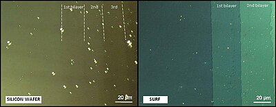
The performance of these supports is evaluated by measuring the contrast (C) of the sample defined as: C = (I1-I0)/(I0+I1) where I0 and I1 represent the intensities reflected by the bare surf and by the analyzed sample on the surf, respectively. For a one nanometer-film thickness, the surfs display a contrast 200 times higher than on silicon wafer.
This high contrast increase allows the visualization with standard optical microscope of films with thicknesses down to 0.3 nanometers, as well as nano-objects (down to a 2 nanometer diameter) and this, without any kind of sample labeling (neither fluorescence, nor a radioactive marker). An illustration of the contrast enhancement is in the Figure for optical microscopy between cross polarizers of a Langmuir-Blodgett structure on a silicon wafer and on a surf.
Applications
[edit]
Life sciences
[edit]Thin films and surface treatment
[edit]Nano-materials
[edit]Commercial applications
[edit]Nanolane's Sarfus Mapping Station is based on surface-enhanced ellipsometric contrast microscopy.[10]
References
[edit]- ^ a b Jones-Bey, Hassaun A. (2006-12-01). "MICROSCOPY: Differential-polarization technique enables precise 3-D nanoimaging". Laser Focus World. Retrieved 2024-11-05.
- ^ Ausserré D; Valignat MP (2006). "Wide-field optical imaging of surface nanostructures". Nano Letters. 6 (7): 1384–1388. Bibcode:2006NanoL...6.1384A. doi:10.1021/nl060353h. PMID 16834416.
- ^ Souplet V, Desmet R, Melnyk O (2007). "Imaging of protein layers with an optical microscope for the characterization of peptide microarrays". J. Pept. Sci. 13 (7): 451–457. doi:10.1002/psc.866. PMID 17559066. S2CID 26078821.
- ^ Carion O, Souplet V, Olivier C, Maillet C, Médard N, El-Mahdi O, Durand JO, Melnyk O (2007). "Chemical Micropatterning of Polycarbonate for Site-Specific Peptide Immobilization and Biomolecular Interactions". ChemBioChem. 8 (3): 315–322. doi:10.1002/cbic.200600504. PMID 17226879. S2CID 1770479.
- ^ Monot J, Petit M, Lane SM, Guisle I, Léger J, Tellier C, Talham DR, Bujoli B (2008). "Towards zirconium phosphonate-based microarrays for probing DNA-protein interactions: critical influence of the location of the probe anchoring groups". J. Am. Chem. Soc. 130 (19): 6243–6251. doi:10.1021/ja711427q. PMID 18407629.
- ^ Yunus S, de Crombrugghe de Looringhe C, Poleunis C, Delcorte A (2007). "Diffusion of oligomers from polydimethylsiloxane stamps in microcontact printing: Surface analysis and possible application". Surf. Interf. Anal. 39 (12–13): 922–925. doi:10.1002/sia.2623. S2CID 93335242.
- ^ Burghardt S, Hirsch A, Médard N, Abou-Kachfhe R, Ausserré D, Valignat MP, Gallani JL (2005). "Preparation of highly stable organic steps with a fullerene-based molecule". Langmuir. 21 (16): 7540–7544. doi:10.1021/la051297n. PMID 16042492.
- ^ Pauliac-Vaujour E, Stannard A, Martin CP, Blunt MO, Notingher I, Moriarty PJ, Vancea I, Thiele U (2008). "Fingering instabilities in dewetting nanofluids" (PDF). Phys. Rev. Lett. 100 (17): 176102. Bibcode:2008PhRvL.100q6102P. doi:10.1103/PhysRevLett.100.176102. PMID 18518311. S2CID 8047821.
- ^ Valles C, Drummond C, Saadaoui H, Furtado CA, He M, Roubeau O, Ortolani L, Monthioux M, Penicaud A (2008). "Solutions of Negatively Charged Graphene Sheets and Ribbons". J. Am. Chem. Soc. 130 (47): 15802–15804. doi:10.1021/ja808001a. PMID 18975900.
- ^ "Sarfus Mapping Nanoscale Microscopy". Photonics Spectra. 8: 31–44. doi:10.2147/NSA.S50042. PMC 4599210. PMID 26491270.

