User:Jiten.meena/Laptop power saving
| This is not a Wikipedia article: It is an individual user's work-in-progress page, and may be incomplete and/or unreliable. For guidance on developing this draft, see Wikipedia:So you made a userspace draft. Find sources: Google (books · news · scholar · free images · WP refs) · FENS · JSTOR · TWL |

Unnecessary signal transitions that do not have any functionality are known as Glitch. Power dissipation of a gate occurs in two ways: Static power dissipation and Dynamic power dissipation. Glitch power comes under dynamic dissipation in the circuit and is directly proportional to switching activity. Glitch power dissipation is 20%-70% of total power dissipation and hence glitch should be eliminated for low power design.
Switching activity occurs due to signal transitions which are of two types: functional transition and a glitch. Switching power dissipation is directly proportional to the switching activity (α), load capacitance (C), Supply voltage (V), and clock frequency (f) as:
- P = α.C.V².f
Switching activity means transition to different levels. Glitches are dependent on signal transitions and more glitches results in higher power dissipation. As per above equation switching power dissipation can be controlled by controlling switching activity (α), voltage scaling etc.
Glitch reduction techniques
[edit]Reducing Switching Activity
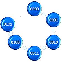
[edit]As discussed, more transition results in more glitches and hence more power dissipation. To minimize glitch occurrence, switching activity should be minimized. For example, in the design of 4 bit counter if gray code is used instead of binary code then switching activity reduces by great extent. As counting from 0000 to 0101, a usual binary counter takes 5 transitions whereas gray code implemented counter takes only 2 transitions and hence switching activity is reduced.

Gate Freezing
[edit]Gate freezing minimizes power dissipation by eliminating glitch. It relies on the availability of the modified library cells so called F-Gate. This methods consists of transforming high glitch gates into modified devices which filters the glitches when proper control signal is applied. When the control signal is high, the F-Gate operates as normal and when control signal is low, the gate output is disconnected from the ground. As a result it can never be discharged to logic 0 and glitch are filtered.
Hazard Filtering and Balanced Path Delay
[edit]Hazards in digital circuits is unnecessary transitions due to different path delays in the circuit. Balanced path delay techniques are used for resolving different path delay problem. To make path delays equal, buffer insertion is done at required paths. Balanced path delay will result in non-glitchy output. Hazard filtering is another way to remove glitch. In hazard filtering gate propagation delays are adjusted. This results in balancing all path delays at the output.
Hazard filtering is preferred over path balancing as path balancing is more energy consuming due to more number of buffer insertion.
Gate Sizing
[edit]Gate upsizing and gate downsizing techniques are used for path balancing. Gate is replaced by logically equivalent but smaller cell so that delay of the gate is changed. Although increasing gate size also increases power dissipation. Hence gate-upsizing is only used when power dissipation by glitch removal is more than power dissipation due to increase in size. Gate sizing affects glitch transition but does not affect functional transition.
Multiple Threshold Transistor
[edit]Delay of each gate is a function of threshold voltage. Non critical paths are selected and threshold voltage of the gates in these paths is increased. This results in balanced propagation delay along different paths converging at the same gate. Performance is maintained as it is determined by critical paths. Higher threshold voltage also reduces leakage current in same path.
See also
[edit]References
[edit]- Hyungoo Lee, Hakgun Shin, Juho Kim, "Glitch Elimination by Gate Freezing, Gate Sizing and Buffer Insertion for Low Power Optimization Circuit" IEEE Transactions 2126-2131. doi: 10.1109/IECON.2004.1432125
- Olivier Coudert, Gate Sizing for Constrained Delay/Power/Area Optimization, IEEE TRANSACTIONS ON VERY LARGE SCALE INTEGRATION (VLSI) SYSTEMS, VOL. XX, NO. Y, SEPTEMBER 1997
- Sachin S. Sapatnekar, Weitong Chuang, Power-Delay Optimizations in Gate Sizing. http://www.ece.umn.edu/~sachin/jnl/todaes00wc.pdf
- Warren Shum and Jason H. Anderson, “FPGA Glitch Power Analysis and Reduction”, International Symposium on Low power electronics and design (ISLPED) 2011, page no. 27-32.
- Zhanping Chen, Liqiong Wei, Kaushik Roy, REDUCING GLITCHING AND LEAKAGE POWER IN LOW VOLTAGE CMOS CIRCUITS, march 1997, Purdue University School of Electrical and Computer Engineering. http://docs.lib.purdue.edu/cgi/viewcontent.cgi?article=1084&context=ecetr
External links
[edit]- Patent US6356101 B1: Glitch Removal Circuitary, 12 Mar 2002, http://www.google.co.in/patents/US6356101.
- https://learn.digilentinc.com/Documents/277
Category:Digital electronics
Category:Electronics optimization
Category:Software bugs
Category:Computer errors

