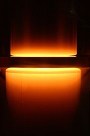
Float-zone silicon


Float-zone silicon is very pure silicon obtained by vertical zone melting. The process was developed at Bell Labs by Henry Theuerer in 1955 as a modification of a method developed by William Gardner Pfann for germanium. In the vertical configuration molten silicon has sufficient surface tension to keep the charge from separating. The major advantages is crucibleless growth that prevents contamination of the silicon from the vessel itself and therefore an inherently high-purity alternative to boule crystals grown by the Czochralski method.
The concentrations of light impurities, such as carbon (C) and oxygen (O2) elements, are extremely low. Another light impurity, nitrogen (N2), helps to control microdefects and also brings about an improvement in mechanical strength of the wafers, and is now being intentionally added during the growth stages.
The diameters of float-zone wafers are generally not greater than 200 mm due to the surface tension limitations during growth. A polycrystalline rod of ultrapure electronic-grade silicon is passed through an RF heating coil, which creates a localized molten zone from which the crystal ingot grows. A seed crystal is used at one end to start the growth. The whole process is carried out in an evacuated chamber or in an inert gas purge.
The molten zone carries the impurities away with it and hence reduces impurity concentration (most impurities are more soluble in the melt than the crystal). Specialized doping techniques like core doping, pill doping, gas doping and neutron transmutation doping are used to incorporate a uniform concentration of desirable impurity.
Float-zone silicon wafers may be irradiated by neutrons to turn it into a n-doped semiconductor.
Application
[edit]Float-zone silicon is typically used for power devices and detector applications, where high-resistivity is required.[1]: 364 It is highly transparent to terahertz radiation, and is usually used to fabricate optical components, such as lenses and windows, for terahertz applications. It is also used in solar arrays of satellites as it has higher conversion efficiency.[2][3][1]: 364
See also
[edit]References
[edit]- ^ a b Sze, S. M. (2012). Semiconductor devices : physics and technology. M. K. Lee (3 ed.). New York, NY: Wiley. ISBN 978-0-470-53794-7. OCLC 869833419.
- ^ "New Solar Innovation Cuts Costs By 60% While Increasing Efficiency By 24%". 19 October 2017. Retrieved 20 October 2017.
- ^ "Float Zone Silicon Solar Panels - 60% less expensive and 25% more efficient". Retrieved 20 October 2017.
- Michael Riordan & Lillian Hoddeson (1997) Crystal Fire: the birth of the information age, page 230, W. W. Norton & Company ISBN 0-393-04124-7 .
