Field effect (semiconductor)

In physics, the field effect refers to the modulation of the electrical conductivity of a material by the application of an external electric field.
In a metal, the electron density that responds to applied fields is so large that an external electric field can penetrate only a very short distance into the material. However, in a semiconductor the lower density of electrons (and possibly holes) that can respond to an applied field is sufficiently small that the field can penetrate quite far into the material. This field penetration alters the conductivity of the semiconductor near its surface, and is called the field effect. The field effect underlies the operation of the Schottky diode and of field-effect transistors, notably the MOSFET, the JFET and the MESFET.[1]
Surface conductance and band bending
[edit]The change in surface conductance occurs because the applied field alters the energy levels available to electrons to considerable depths from the surface, and that in turn changes the occupancy of the energy levels in the surface region. A typical treatment of such effects is based upon a band-bending diagram showing the positions in energy of the band edges as a function of depth into the material.
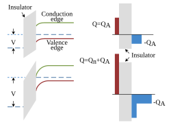
An example band-bending diagram is shown in the figure. For convenience, energy is expressed in eV and voltage is expressed in volts, avoiding the need for a factor q for the elementary charge. In the figure, a two-layer structure is shown, consisting of an insulator as left-hand layer and a semiconductor as right-hand layer. An example of such a structure is the MOS capacitor, a two-terminal structure made up of a metal gate contact, a semiconductor body (such as silicon) with a body contact, and an intervening insulating layer (such as silicon dioxide, hence the designation O). The left panels show the lowest energy level of the conduction band and the highest energy level of the valence band. These levels are "bent" by the application of a positive voltage V. By convention, the energy of electrons is shown, so a positive voltage penetrating the surface lowers the conduction edge. A dashed line depicts the occupancy situation: below this Fermi level the states are more likely to be occupied, the conduction band moves closer to the Fermi level, indicating more electrons are in the conducting band near the insulator.
Bulk region
[edit]The example in the figure shows the Fermi level in the bulk material beyond the range of the applied field as lying close to the valence band edge. This position for the occupancy level is arranged by introducing impurities into the semiconductor. In this case the impurities are so-called acceptors which soak up electrons from the valence band becoming negatively charged, immobile ions embedded in the semiconductor material. The removed electrons are drawn from the valence band levels, leaving vacancies or holes in the valence band. Charge neutrality prevails in the field-free region because a negative acceptor ion creates a positive deficiency in the host material: a hole is the absence of an electron, it behaves like a positive charge. Where no field is present, neutrality is achieved because the negative acceptor ions exactly balance the positive holes.
Surface region
[edit]Next the band bending is described. A positive charge is placed on the left face of the insulator (for example using a metal "gate" electrode). In the insulator there are no charges so the electric field is constant, leading to a linear change of voltage in this material. As a result, the insulator conduction and valence bands are therefore straight lines in the figure, separated by the large insulator energy gap.
In the semiconductor at the smaller voltage shown in the top panel, the positive charge placed on the left face of the insulator lowers the energy of the valence band edge. Consequently, these states are fully occupied out to a so-called depletion depth where the bulk occupancy reestablishes itself because the field cannot penetrate further. Because the valence band levels near the surface are fully occupied due to the lowering of these levels, only the immobile negative acceptor-ion charges are present near the surface, which becomes an electrically insulating region without holes (the depletion layer). Thus, field penetration is arrested when the exposed negative acceptor ion charge balances the positive charge placed on the insulator surface: the depletion layer adjusts its depth enough to make the net negative acceptor ion charge balance the positive charge on the gate.
Inversion
[edit]The conduction band edge also is lowered, increasing electron occupancy of these states, but at low voltages this increase is not significant. At larger applied voltages, however, as in the bottom panel, the conduction band edge is lowered sufficiently to cause significant population of these levels in a narrow surface layer, called an inversion layer because the electrons are opposite in polarity to the holes originally populating the semiconductor. This onset of electron charge in the inversion layer becomes very significant at an applied threshold voltage, and once the applied voltage exceeds this value charge neutrality is achieved almost entirely by addition of electrons to the inversion layer rather than by an increase in acceptor ion charge by expansion of the depletion layer. Further field penetration into the semiconductor is arrested at this point, as the electron density increases exponentially with band-bending beyond the threshold voltage, effectively pinning the depletion layer depth at its value at threshold voltages.
References
[edit]- ^ The acronyms stand for Metal Oxide Semiconductor Field Effect Transistor, Junction Field Effect Transistor, and MEtal Semiconductor Field Effect Transistor. For a discussion see, for example, M K Achuthan K N Bhat (2007). "Chapter 10: Metal semiconductor contacts: Metal semiconductor and junction field effect transistors". Fundamentals of semiconductor devices. Tata McGraw-Hill. pp. 475 ff. ISBN 978-0070612204.
This article incorporates material from the Citizendium article "Field effect#Field effect", which is licensed under the Creative Commons Attribution-ShareAlike 3.0 Unported License but not under the GFDL.
