Cathode follower oscillator
This article needs additional citations for verification. (March 2024) |


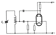
The Cathode follower oscillator is an electronic oscillator circuit in which the oscillation frequency is determined by a tuned circuit consisting of capacitors and inductors, that is, an LC oscillator.[1] The circuit is also known as differential amplifier oscillator, emitter follower oscillator, source-coupled oscillator or Peltz oscillator.[2][3] This oscillator uses one connection to get a signal from the LC-circuit and feeds an amplified signal back. The amplifier is a long-tail pair of two triodes, two bipolar transistors or two junction FETs.
Operation
[edit]In the Cathode follower oscillator schematic, the long tail amplifier is connected to a tap of the LC-circuit inductance for a light load on the LC-circuit. A grid-leak couples the grid of the left triode to the LC-circuit. The left triode uses common anode circuit which has high input impedance, low output impedance and no voltage amplification. The long-tail resistor couples the two triodes. The right triode uses common grid circuit which has low input impedance, high output impedance and no current amplification. A capacitor at the anode resistor of the right triode couples the amplified signal back to the LC-circuit. At low frequency, both triodes have a phase shift of zero degree.
The Peltz oscillator schematic uses PNP transistors. The LC-circuit L1, C1 is connected to the base of the left transistor (Q1) and to the collector of the right transistor (Q2). Q1 is configured as an emitter follower (common-collector) and Q2 is configured as a common-base amplifier, providing voltage gain. The emitter follower is coupled to the common-base amplifier through the long-tail resistor R1, providing net gain necessary for oscillation. Oscillation frequency is around 10 MHz with the components shown. The circuit is optimized for low supply voltage and can operate down to around 0.8V [4]. The voltage across the tuned circuit is approximately ±Vbe peak relative to ground.
The source-coupled oscillator uses two junction FET and a LC-circuit to produce a sine wave signal. L1 and C1 are the LC-circuit, J1 is a common drain amplifier, J2 is a common gate amplifier. The grid-leak C2, R2 connects the LC-circuit to J1 input. J1 output is directly connected to J2 input. The long-tail resistor R1 works as a primitive current source. If the current through J1 increases, the current through J2 decreases. The LC-circuit is directly connected to J2 output. The circuit is optimized for low supply voltage.
References
[edit]- ^ Jiri Vackar, LC Oscillators and their Frequency Stability, Fig. 7, Tesla Technical Reports, Praha, December 1949
- ^ Günter Peltz, Zweipolige Oszillatorschaltungen für Parallel- und Serienresonanz, Funkschau, 1971, Heft 15, S. 465–466
- ^ Koster, Waldow, Wolff, A unique, low-voltage, source-coupled J-FET VCO, RF signal processing, April 2001
- ^ Simple 5-component oscillator works below 0.8V
